Check against your limits.
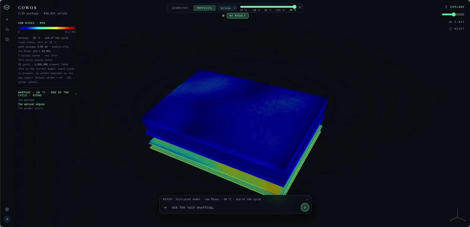
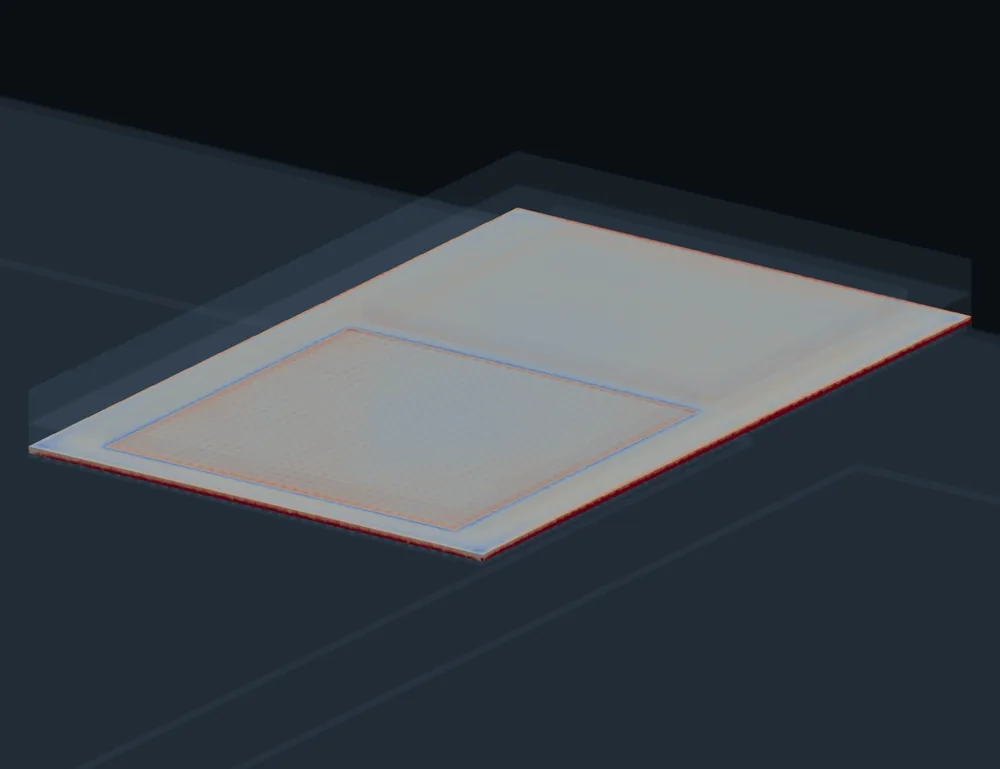
Inspect package deformation through the relevant thermal and process conditions.
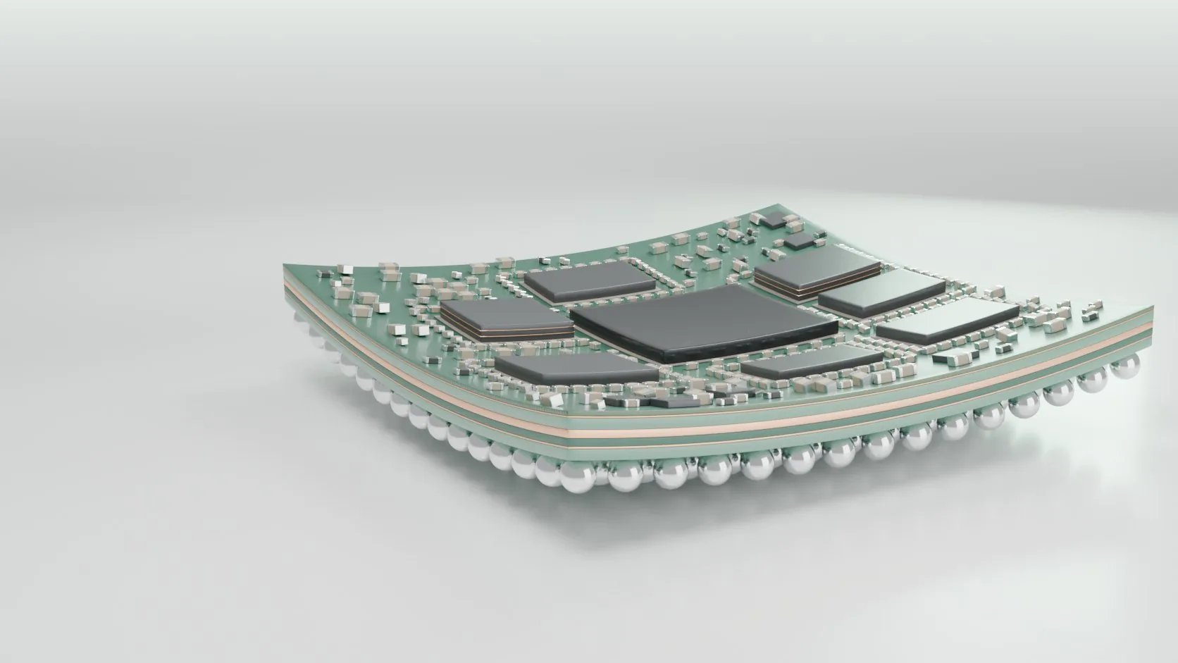
Warpage exaggerated for illustrative purposes.
Package warpage, and the stress, alignment and optical performance it drives, predicted across physics and scales in a Physics Twin built for your package.
Heat changes shape. Shape builds stress in every layer and every solder joint. Resolving that thermal and structural response, from micrometer-scale joints to the full package, can overwhelm conventional compute.


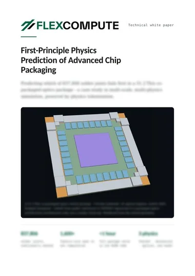
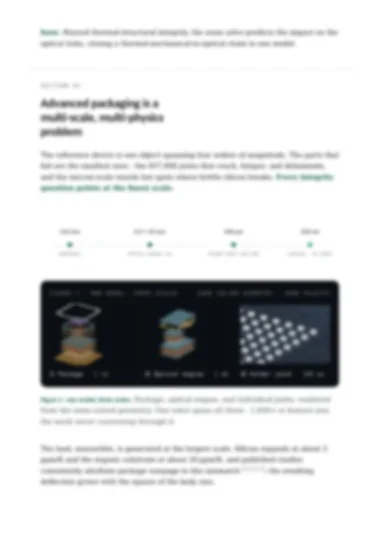
One package. Three scales, from centimeters to micrometers, in one model. The green box marks the region shown next.
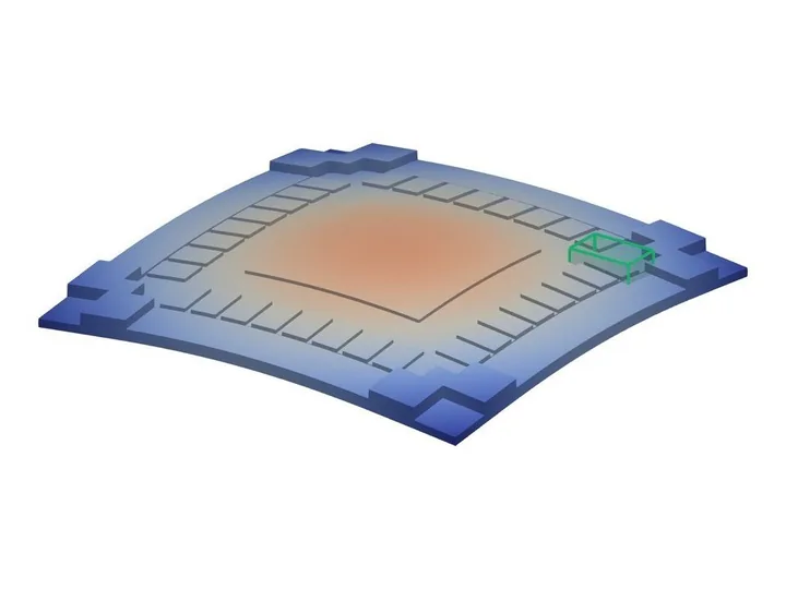
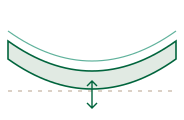
Different materials expand by different amounts, so the whole assembly warps.
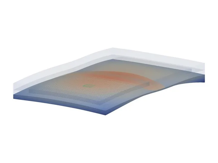
Each layer expands at its own rate, building stress where the layers meet.
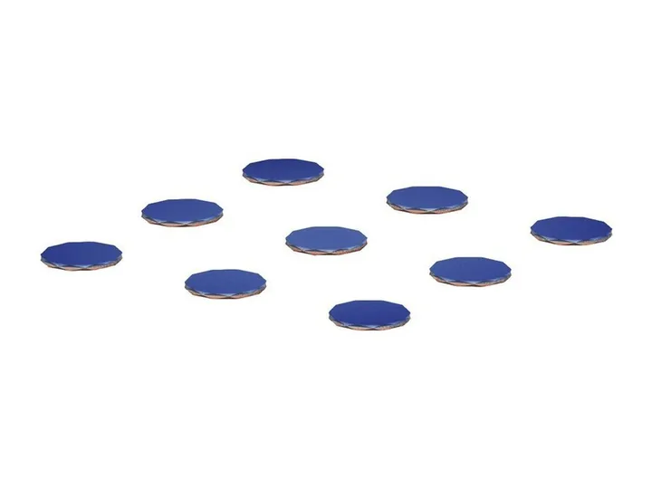
Package warpage loads every joint. Small, repeated strains decide which one fails first.

Simplify the model, risk missing what matters. Average away fine features, isolate components or drop a physical effect, and you can lose the interaction that determines whether the package works.
Simulation renders from one full-package model; warpage exaggerated for illustration. Reference architecture reconstructed from public Spectrum-X co-packaged optics and COUPE information.
Watch a Physics Twin find the first solder joint to fail under thermal cycling, and when, before a single part is built.
Keep the physics that matters. Make the computation practical.
| Aspect | Traditional computer-aided engineering (CAE)Fit the problem to the tools. | Tokenized PhysicsFit the model to your problem. |
|---|---|---|
| Turnaround | Prohibitive at full detailThe reference package is estimated at a million graphics processing unit (GPU) hours by direct finite element analysis. | 30 minutesReported full-package solve on 8 NVIDIA B200 GPUs, with detail retained. |
| Physics | One discipline at a timeSeparate models, transferred loads and results to reconcile. | Relevant physics, connectedA shared package context, with couplings scoped to your design. |
| Scale | Full package or fine detailAverage small features or isolate a few regions to keep the model manageable. | Full package and fine detailResolve local response within the full-package model. |
| Fidelity | Simplify to make it solvableEffective layers, selected submodels or ray approximations. | Full geometry, full-wave fieldsMechanics and optics solved from the governing equations. |
110 mm package. Full layers and fine interconnect geometry.
1.24 mm optical path. Full-wave propagation, end to end.
Reference-case results, not a guaranteed runtime for every design. GPU-hours measure total compute; 4 GPU-hours on 8 B200 GPUs is 30 minutes of elapsed solve time. Conventional costs are estimates, not measured runs on identical hardware. Source: Flexcompute, Semicon Taiwan presentation.
Replay the assembly sequence to see when stress develops. In this example, underfill cure leaves substantial die stress before thermal cycling even begins.
By underfill cure, the die already carries roughly two-thirds of its later cold-cycle peak stress—at room temperature, before thermal cycling.
Identify which assembly step to change before the next build.
Separate full-package reference model. Inspect local deformation with the surrounding assembly still included.
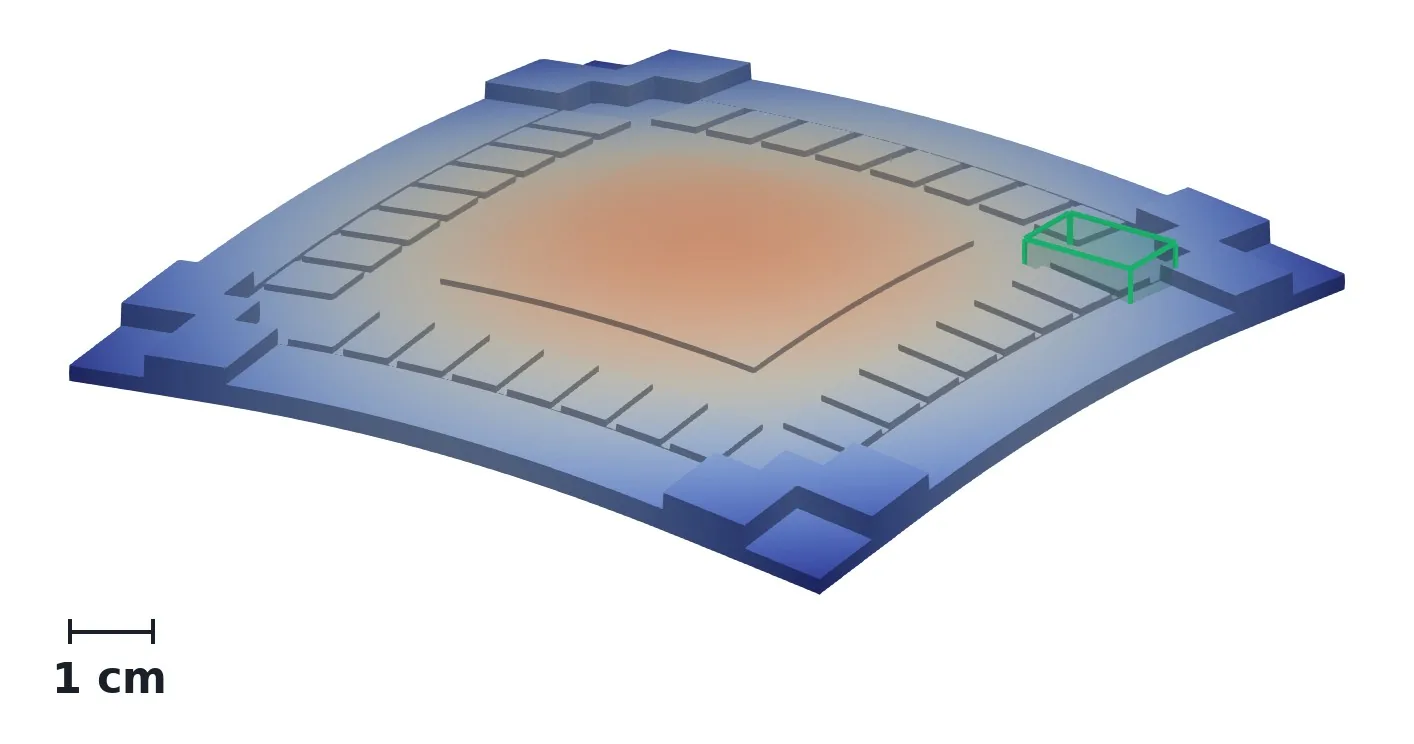
Inspect deformation across the entire assembly. All four solder levels, 12 embedded bridges, and the substrate layers are included in this model.
The manufacturing sequence models one optical engine. Stress values are read at the end of each step, at 20 °C except the −40 °C cold extreme. Figure colors are clipped to ±25 MPa; the reported peaks come from element values. The expandable warpage views show a separate full-package reference solve, reconstructed from public NVIDIA Spectrum-X co-packaged optics architecture information rather than a vendor stack-up. Deformation magnification is labeled in each view.
These examples cover thermal loading and structural response. Local stress and strain support investigation under the stated model conditions; predicting cycles to failure requires an appropriate fatigue model and validation. Material inputs, boundary conditions, accuracy criteria, and modeling assumptions are reviewed during setup. Get the white paper
From First-Principle Physics Prediction of Advanced Chip Packaging.

Know which one fails first.

On an 8-GPU NVIDIA B200.
From a 100 µm joint to a 110 mm package, without coarsening the mesh.
For comparison: published models that simplify the joint arrays carry about 60% error in per-cycle creep strain, and cannot reliably locate the worst-case joint.
faster than legacy solvers
more of the design cycle, saving time and cost

Validation against the laws of physics, fast enough to keep pace with artificial intelligence (AI) in advanced manufacturing.
Every industry is racing to put AI to work on real engineering problems, and the limit is how quickly each one can be validated against the laws of physics. Flexcompute has built something unique: simulation fast enough to keep pace with AI and rigorous enough for production decisions. In advanced manufacturing, that means more of the design cycle happens digitally, saving time and cost.
Investigate package response before committing to the next build. Use the result to focus material, geometry, and process changes.
Inspect package deformation through the relevant thermal and process conditions.
Locate vulnerable regions and the assembly steps that contribute to their stress.
Explore material, geometry, and process changes within the same configured workspace.
 Which of 837,806 solder joints fails first, and how much margin each one hasHow a coupled solver carries a 110 mm package down to its 100 µm joints in one computationHow thermal, mechanical and optical results come from one model, step by step through manufacturing
Start with your package architecture and the question you need to answer. Available geometry, stack-up, material data, process temperatures and engineering limits help establish the scope. We can identify missing inputs together.
The engagement starts with expert guidance. Together, we define the physical model, review available inputs and configure the views around your decisions. The goal is a workspace your team can keep using; the setup effort is scoped around your design.
That is the product's purpose. Explore questions and compare changes within the configured scope. When a new material, process or physical effect changes that scope, review the model and assumptions with the team.
Open the white paper, First-Principle Physics Prediction of Advanced Chip Packaging, for the source figures and modeling context. The full-package result and the single-engine manufacturing sequence have separate scopes.